- TOP
- Products
- Test Solutions Business
- Burn-in Sockets
Burn-in Sockets
Burn-in sockets are for the accelerated testing of semiconductors subjected to temperature and voltage loads. We offer burn-in sockets for various packages, such as ball grid array (BGA), land grid array (LGA), quad flat pack non-lead (QFN), and small outline non-lead (SON) packages. We also have a lineup of heat sinks and heater sensors.
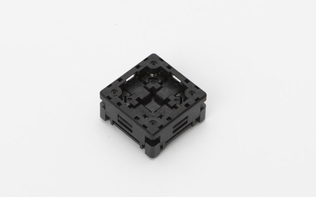
open top
Burn-in sockets for mass production enable automatic insertion and removal of semiconductors and are compatible with a wide range of package thicknesses.
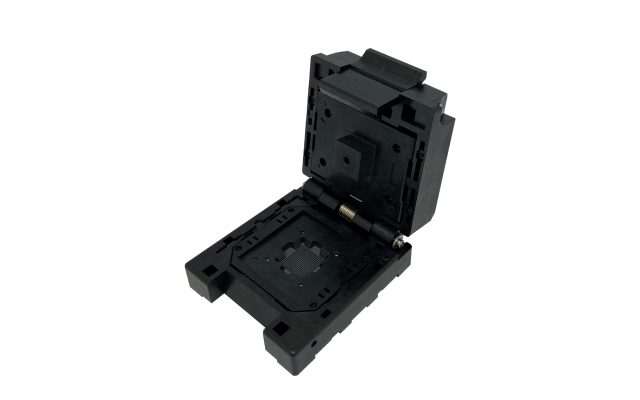
clamshell
We offer solutions for high-mix, low-volume applications. Low-inductance sockets with a self-inductance 1nH or less are available, and we also have a lineup of heat sinks and heater sensors.
others
Single-in-line-package (SIP), dual in-line package (DIP), and zig-zag in-line package (ZIP) sockets are lined up. Highly reliable double-sided movable two-point contacts are used.
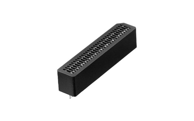
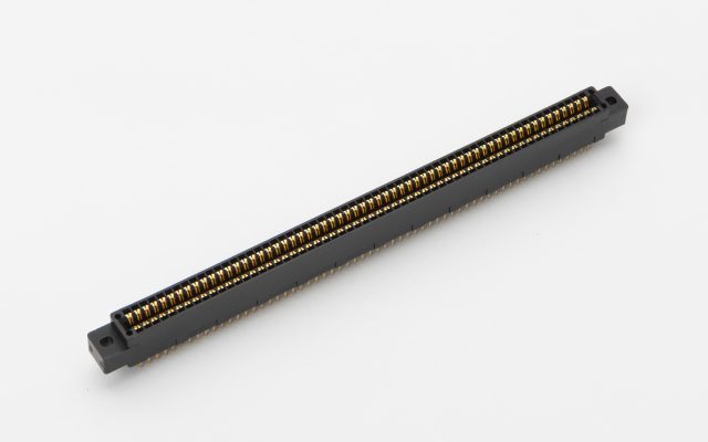
cardedge
Card edge connectors are for PCB connections used for burn-in devices. The excellent contact structure provides high durability and contact reliability.